Бор: от базового материала до высокотехнологичного ядра. Анализ прецизионного применения высокочистого бора в полупроводниках и передовых областях
В высокотехнологичных областях, стремящихся к микроскопическим пределам и высочайшим показателям производительности, определённые фундаментальные элементы играют решающую роль. Бор, элемент с обозначением B и атомным номером 5, — один из таких элементов. Этот металлоид, встречающийся в природе только в виде соединений, стал незаменимым «ключевым элементом» в таких областях, как полупроводники, передовые материалы и атомная промышленность, благодаря своей уникальной электронной структуре и физико-химическим свойствам.
1. «Мастера своего дела» полупроводниковой промышленности: прецизионное легирование и выращивание кристаллов
В полупроводниковой промышленности ценность высокочистых кристаллических бор заключается в его непревзойденных возможностях точности управления.
Краеугольный камень легирования P-типа: бор используется в основном как легирующая примесь P-типа. Кремний (Si) — бесспорный «рабочий конь» полупроводниковых материалов, но по своей природе он обладает плохой проводимостью. При точной имплантации атомов бора в решётку кремния такими методами, как ионная имплантация или высокотемпературная диффузия, внешняя оболочка бора содержит всего три электрона, в то время как у кремния их четыре. Это создаёт «дырку», способную вмещать и переносить электроны, фактически создавая полупроводник P-типа. Этот процесс «легирования» лежит в основе построения PN-перехода — основного структурного элемента всех полупроводниковых приборов, включая диоды, транзисторы и тиристоры.
Ключ к силовым устройствам и масштабированию: в силовых устройствах, которые должны выдерживать высокие напряжения и токи (например, IGBT и силовые МОП-транзисторы), кремниевые пластины, легированные бором (обычно в области высокого сопротивления), эффективно регулируют распределение электрического поля и повышают выдерживаемое напряжение устройства. Кроме того, в современных технологических узлах формирование сверхмелких переходов требует чрезвычайно высокой точности легирования. Бор, благодаря своему малому атомному радиусу, обеспечивает более точный контроль легирования, отвечая требованиям наноразмерных устройств.
Исходный материал для выращивания монокристаллов: Помимо легирования, кристаллический бор также используется в качестве исходного материала для выращивания легированных бором кремний Монокристаллы, полученные методом плавления. Этот метод позволяет получать слитки кремния с равномерной проводимостью P-типа по всей пластине, что закладывает основу для крупномасштабного производства высокостабильных полупроводниковых приборов.
2. За пределами полупроводников: выдающиеся характеристики бора во многих областях
Применение бора выходит далеко за рамки полупроводников: его соединения и изотопы находят применение во многих передовых областях.
Современные конструкционные материалы: Чрезвычайно высокая твёрдость бора (9,5 по шкале Мооса) делает его идеальным армирующим материалом. Борные волокна и боридная керамика являются ключевыми компонентами в производстве высокопрочных и лёгких композитных материалов, широко используемых в аэрокосмической промышленности, производстве высокопроизводительного спортивного оборудования и других областях.
Специальное стекло и керамика: В производстве стекла добавление оксида бора значительно снижает коэффициент теплового расширения, обеспечивая отличную стойкость к тепловым ударам. Это боросиликатное стекло является предпочтительным выбором для лабораторной посуды (например, термостойких стаканов) и высококачественной кухонной посуды. Аналогичным образом, добавление соединений бора в керамику повышает её термостойкость и механическую прочность.
Захват нейтронов и ядерная промышленность: природный бор содержит около 20% изотопа бора-10, обладающего чрезвычайно высоким сечением захвата тепловых нейтронов. Это свойство делает бор-10 (обычно в форме карбида бора или борной кислоты) незаменимым материалом для стержней управления, нейтронной защиты и защитного агента в системах аварийного отключения ядерных реакторов.
Органический синтез и фармацевтика: В области тонкой химии и фармацевтики борсодержащие реагенты (такие как бороновые кислоты и бороновые эфиры) являются важными промежуточными продуктами для образования углерод-углеродных и углерод-гетероатомных связей, особенно в реакциях сочетания Сузуки-Мияуры. Всё больше борсодержащих органических молекул разрабатываются в качестве новых фармацевтических препаратов. Например, некоторые ингибиторы протеасом стали важными средствами противораковой терапии.
3. Качество — краеугольный камень технологии: надежные поставки из Китая
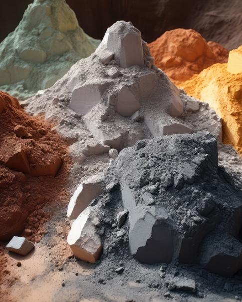
В связи с такими обширными и сложными высокотехнологичными приложениями требования к чистоте, однородности и конкретной форме (например, размеру частиц и форме кристаллов) борсодержащих материалов достигли беспрецедентного уровня.
Компания UrbanMines Tech., ведущий производитель и поставщик высокочистых борсодержащих материалов в Китае, глубоко осознаёт решающее влияние свойств материалов на конечную продукцию. Используя собственные контролируемые производственные линии, мы специализируемся на поставках высокочистого кристаллического и аморфного бора полупроводникового качества, а также различных соединений бора по индивидуальному заказу клиентам по всему миру.
Мы твёрдо убеждены, что только самые передовые продукты могут соответствовать требованиям передовых технологий. Поэтому мы стремимся к тесному сотрудничеству с глобальными партнёрами в области НИОКР и производства, чтобы совместно расширять границы технологий — от микросхем до чистой энергии, предлагая высокопроизводительные, стабильные и надёжные решения на основе борсодержащих материалов.


 IPv6 ПОДДЕРЖИВАЕМАЯ СЕТЬ